Photovoltaic modules and solar collectors
Photovoltaic modules and solar panels have taken the European market by storm. Their perfect processing makes a big difference in the performance of the final products. Consequently, the efficiency of silicon wafers means energy efficiency and energy savings for the user. At KK SOLUTIONS, we know how important the processing of photovoltaic wafers is.
That's why, with exateq GmbH, we offer equipment that is perfectly tailored to our customers' expectations!
Processing of photovoltaic wafers - what is involved?
Before silicon chunks become a suitable semiconductor, they have to go through a series of processes. The first involves pulling crystals from the chunks at high temperatures. Already at this early stage, boron or phosphorus is added to the silicon to give the wafers the required semiconductor character. The drawn single crystals are cut (sawn) into slices (wafers). The wafers can vary in size and thickness, the latter being no more than a fraction of a millimeter.
The size can also vary and subsequently determines how large the finished photovoltaic panels are for which the wafers are needed. Finally, the wafers are inspected to determine dimensional conformance, the extent of any contamination, and an overall assessment of the wafer's suitability. Wafers that do not pass this inspection are recycled.
KK SOLUTIONS and equipment for processing photovoltaic wafers
The silicon wafers cut in this way are then further processed into solar cells. In this process, surfaces damaged by cutting must be removed (etched) in order to roughen them so that they absorb as much light as possible. They are then cleaned of impurities and., pass through the next production process.
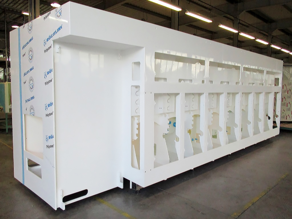
exateq GmbH designs the equipment required for this and then, together with KK SOLUTIONS, builds wet-chemical processing systems for customers that ensure precise processing of PV wafers.
The importance of texturing and doping processes
These two processes are critical to the performance and functionality of photovoltaic modules. In the first method - texturing - silicon wafers are dipped into a hot solution of sodium hydroxide mixed with special additives. Monocrystalline wafers, and ultimately the panels, are textured in this way, leaving their surface dotted with tiny pyramids. This process drastically increases the absorption of solar energy, which manifests itself in the dark color. If the surface were completely flat, the panel would strongly reflect the light instead of converting it into electricity.
In doping, wafers are placed in furnaces with an atmosphere of boron or phosphorus and heated to high temperatures (about 800 °C). This process creates a layer with a different electrical potential. After doping, the wafer is subjected to plasma treatment in particular, which further increases the efficiency.
Choose a fruitful cooperation with Exateq GmbH and KK SOLUTIONS!
The production of equipment for the manufacture and processing of wafers is one of the specialties of exateq GmbH and KK SOLUTIONS. We at KK SOLUTIONS know how important quality is while reducing production costs. That is why we focus on direct contact with the customer to generate solutions that are tailored to the expectations and needs of the user.
Contact us now and start a satisfying cooperation with us. We guarantee an individual approach to each project and the highest level of satisfaction with the result. See for yourself how fruitful our cooperation can be and ensure the highest quality of your solar wafer and cell manufacturing equipment!